The BlitzenKlavier
Humans of the internet, I present to you the BlitzenKlavier (lightning-piano). It’s a large solid-state Tesla coil that takes in 120VAC, MIDI, and spits out 8 foot musical lightning bolts!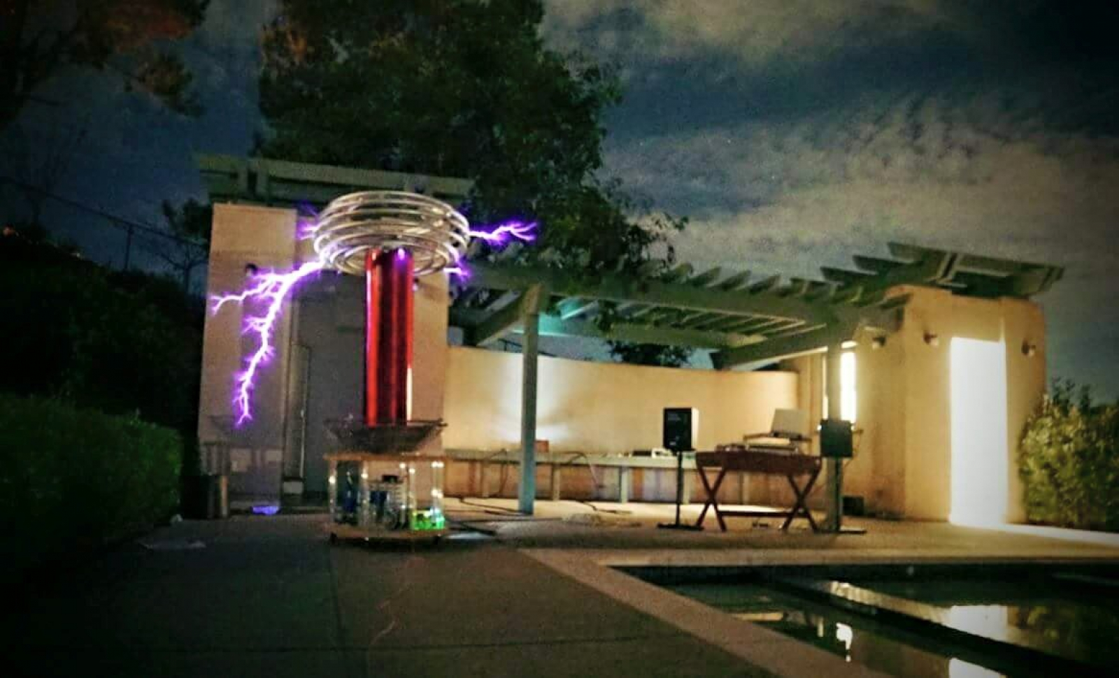
 Slowly, the rising and falling magnetic field begins to create an oscillation in the secondary, high voltage tank, one which eventually builds up enough potential to ionize the air surrounding the coil’s top-mounted torus, setting free some electrons which make it their mission to find the nearest grounded object.As simple a circuit as they may be, it’s hard to not admire a coil’s elegance. But we can do better than this now; we have the technology!Within the past decade, power semiconductor manufacturers have made great strides. Where it once cost a small fortune to electronically switch 50 amperes, it’s now possible to switch thousands of amps, in shorter amounts of time, with less loss than ever before.In fact, with IGBTs [insulated-gate bipolar transistor] capable of switching an entire city block at 50kHz available for only a few hundred dollars, it becomes feasible now to build solid state Tesla coil.But how?
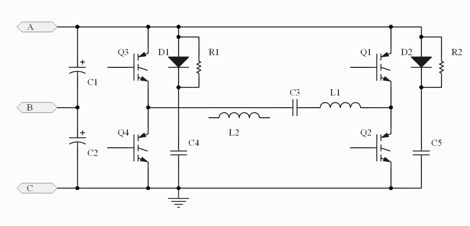 Being an H bridge, there is nothing all that special about the design. A bus capacitance, C1 & C2 provides 280V across the IGBTs and in my case, is capable of supplying 1.3kJ in a few milliseconds if needed. C3 & L1 constitute the primary tank, composed of the Tesla coil’s primary, and an array of polypropylene capacitors.In order to ensure proper timing, a current transformer, L2, spies on the primary tank’s oscillation. When the current in the primary crosses zero, the IGBTs are switched. By ensuring that switching only occurs when no power is being dissipated by the transistors, the LC tank is free to run at its own natural frequency, rather than being forced into an oscillation which makes the IGBTs unhappy; possibly explosively unhappy.However, zero current switching in a bridge this large is never always zero, so two snubber capacitors are employed across the bus to protect the transistors. If, for some reason a large current flow is interrupted, and the tank inductance fights back, the rising voltage on the bus will be stopped by a low impedance, 1.5uF PP capacitor.Very quick transients are not clamped by the snubber diode though, which may be unbiased for some good amount of time per cycle. To compensate for this, a 5 ohm resistor is placed in parallel with the diode, to help the snubber function until the diode has gone through its reverse recovery delay.As simple as the bridge may sound though, there’s a lot more to it than initially meets the eye.
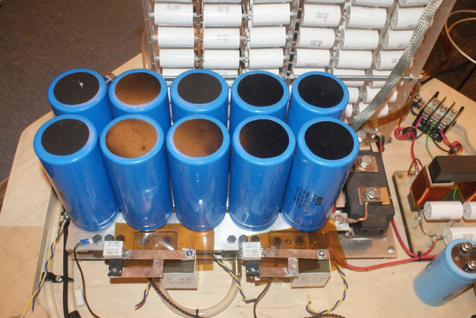 In an LC tank which might see 1kV @ 1000A RMS, one needs a very sturdy, almost indestructible capacitor. For this reason a large safety margin should be employed, up to 3X the expected voltages and currents for good measure.Now, 12kV 0.6uF capacitors aren’t exactly a standard component; especially ones which will see 100% voltage reversal at 40kHz! The only practical option then, is to create a series-parallel bank of smaller capacitors, ones that when combined, will sum to the ratings we’re looking for.For this, the Cornell Dubilier 942C20P15K-F polypropylene snubber capacitor has proven to be the component of choice. It’s just a standard low inductance, self-healing metalized capacitor, but unlike most PP caps, the 942C has foil plates interleaved with the metalized PP surfaces for extra current handling capability. In fact, they are rated for a dV/dt of 2879 V/uS, which, when multiplied by 0.6uF gives a maximum current handing capability of 1727 Amperes.By stringing six capacitors in series and 24 strings in parallel, a 0.6uF, 3000VAC, 1700A self-healing tank capacitor, perfect for the task at hand.
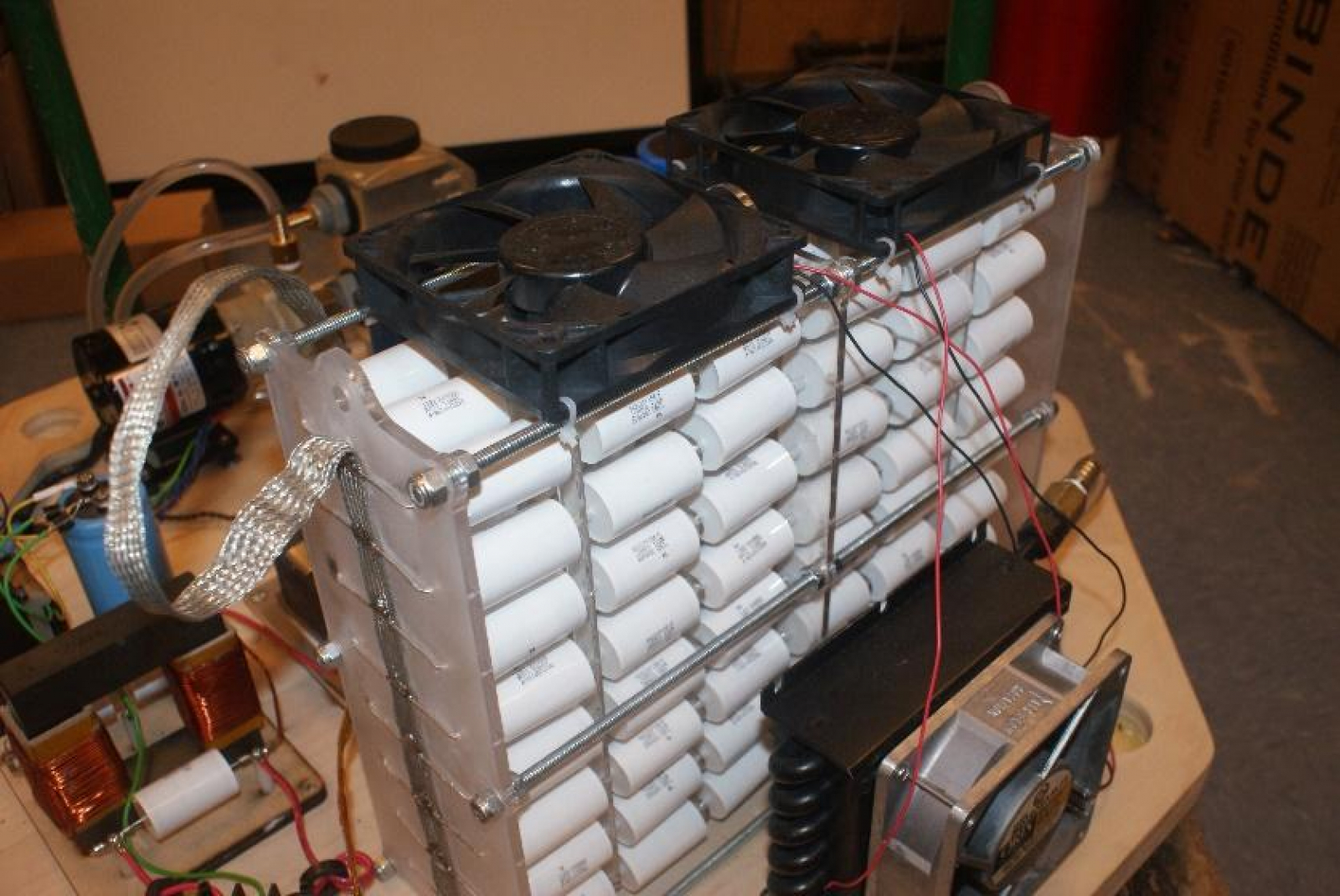 Some care must also be taken when busing such a capacitor, also. To ensure that the currents are equally distributed across the bank, one should ensure that if a connection is made from the top of one side of the bank, the other is made from the bottom. This equalizes the DC resistance, guaranteeing that no group of capacitors is hogging a majority of the electrons.
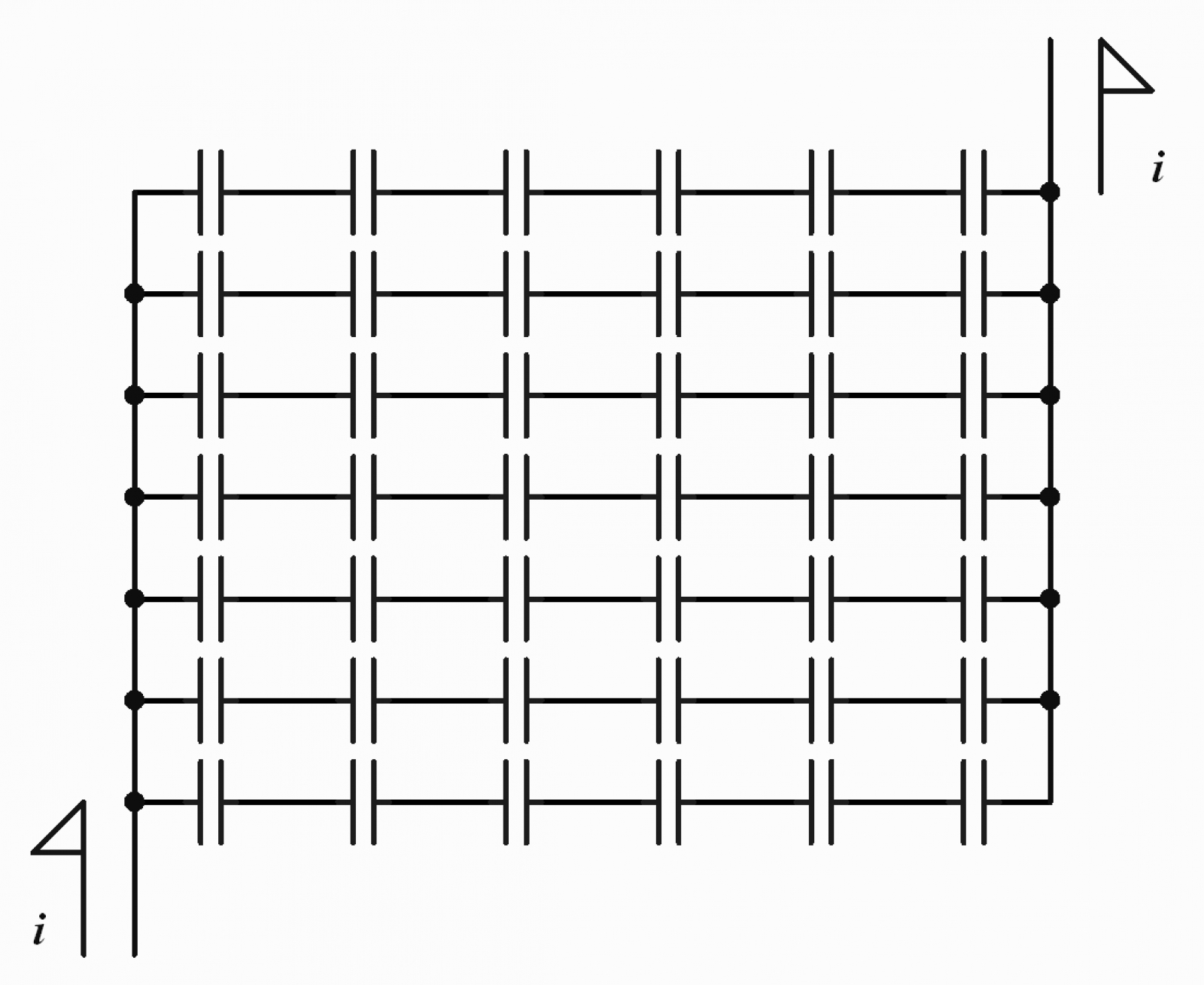
 To ensure the best possible operation of the H-bridge, the transistors are actively kept chilled via a circulating water system. Though the cooling blocks are little else than s-grooves cut into aluminum blocks & welded to a base plate, it works well for the application, and is efficient.
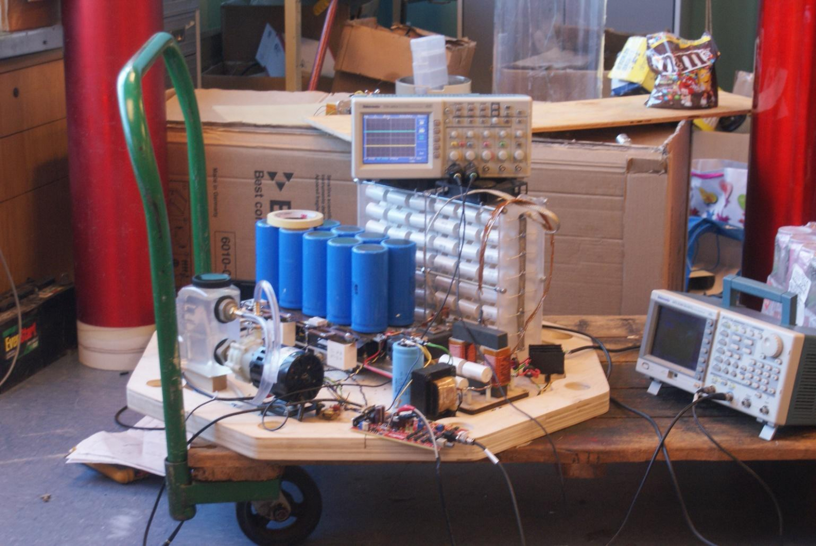
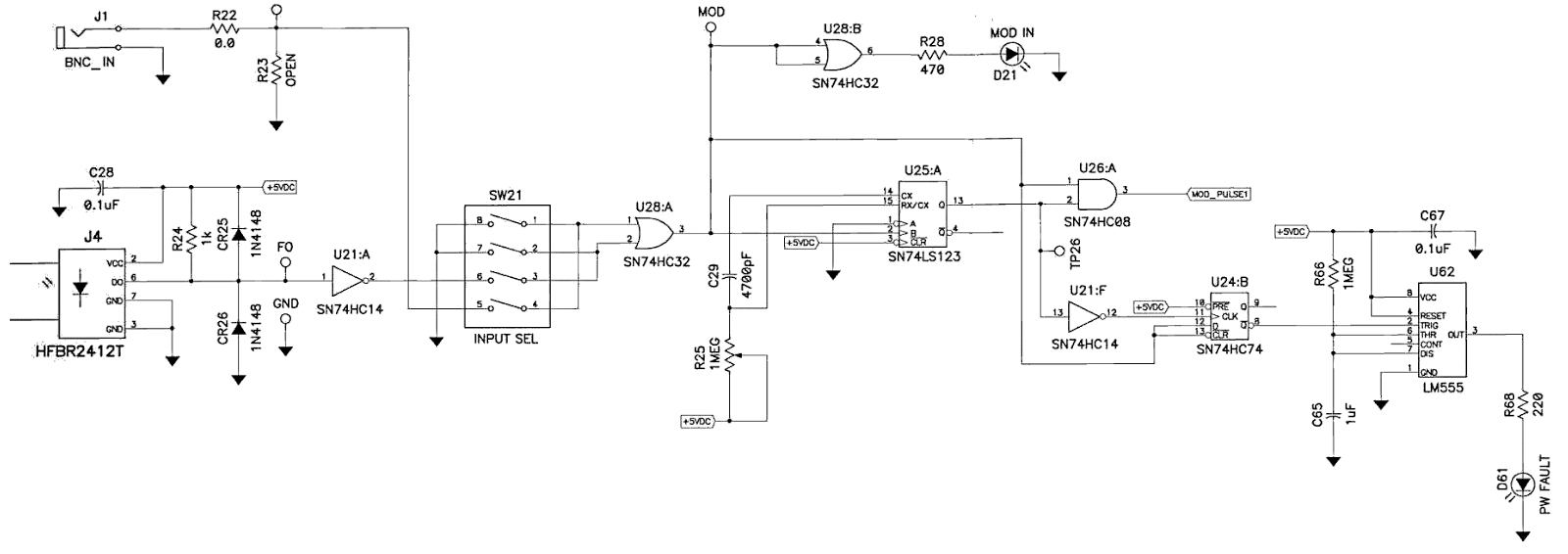 A control pulse, optical or electrical respectively arrives to either J4 or J1, from a computer, instrument or a microcontroller. The pulse needn’t be special, it just needs to be no longer than a few microseconds, since its length is what determines the length of the tank’s oscillation.If optical, the pulse undergoes some conditioning before being sent through a dip switch and into an OR gate. For convenience, the dip switch lets one easily determine what sort of signal the rest of the logic is able to respond to.For debugging purposes, the pulse is buffered and sent into D21, where through a different path it also arrives at both a SN74LS123 multivibrator and at ¼ of a SN74HC08 AND gate. It’s not wise to assume that the incoming pulse is of a safe width, so these two logic functions ensure that the pulse is never longer than the one set via R25. If it is, the SN74HC74 flip-flop & 555 timer will illuminate D61 for a bit to let the operator know that their pulse is being clipped.The conditioned pulse is then sent off to this section:
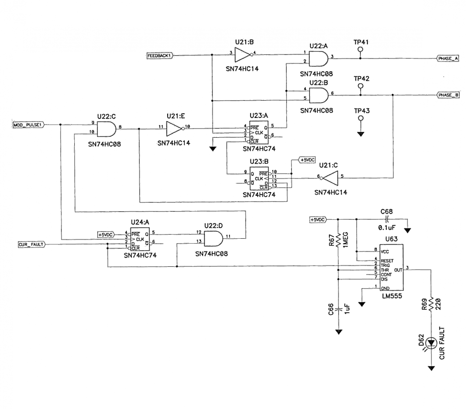 Here, the pulse arrives at another SN74HC08 AND gate, along with a current fault signal we’ll discuss later. If the universe is all happy then there should be no current fault, and the signal makes it through to the ‘D’ input of one SN74HC74 flip-flop, and the preset line of another after passing through a SN74HC14 inverter. If “FEEDBACK 1” is low, (it should be, at this point) then U23:A sets its output high, which brings high the output of U22:A, another and gate. “PHASE_A” is then brought high, while “PHASE_B” is clamped low by U22:B and the currently low “FEEDBACK 1” signal. Both then wander off the page into...
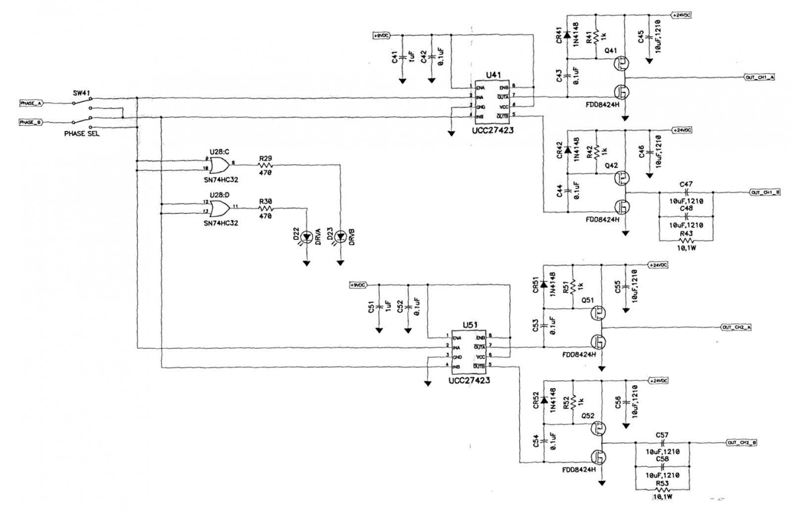 Here, both “PHASE A” and “PHASE B” are greeted by a dip switch which allows for easy phase shifting, if need be. They are then buffered, sent into LEDs and forwarded into UCC27423 gate driver ICs. Following “PHASE A”, it becomes apparent that the UCC27423 will output two complementary signals, which themselves are fed into an N channel mosfet. A P channel fet is placed in series, and the signal is then free to pass through a capacitor to bring low the normally high gate. “PHASE A” is now amplified, and ready to be sent into a big ‘ol gate drive transformer.The bridge then switches! Now with two transistors turned on, a massive current flows into the tank from the bus capacitors and the current transformer begins to output the beginnings of a sine wave. This transformer is in actuality, a cascade of transformers. To ensure a very low sensitivity, one large CT of turns ratio 33:1 is fed into a smaller CT, having a turns ratio of 33:1. With the signal from the 1:1089 current transformer now available, it becomes possible to continue the oscillation.Two separate small cores, instead of one, are used for better noise reduction.
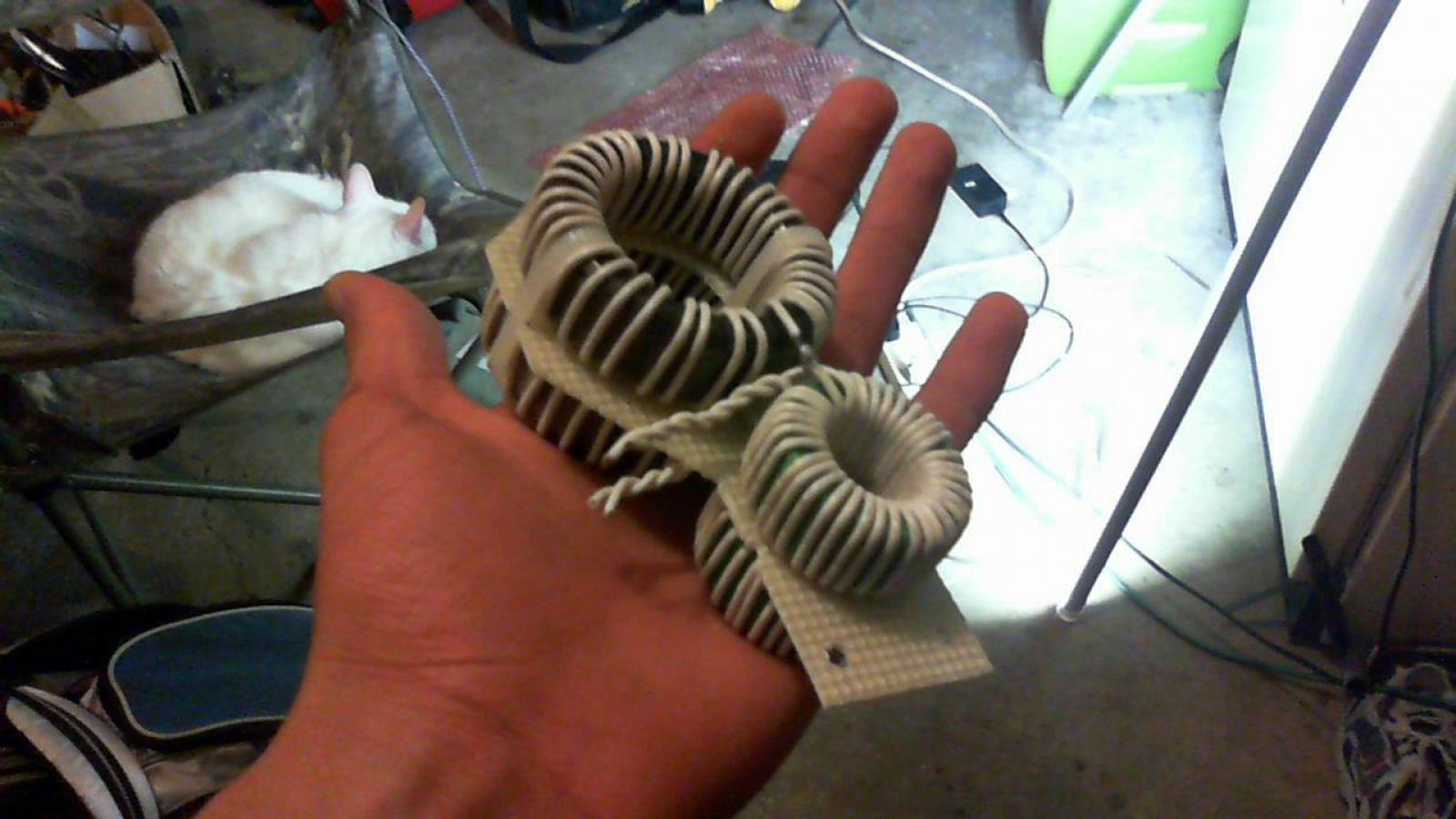 One of these signals makes its way back to the control board and is rectified, clamped and fed into an inverter, where the signal leaves the diagram as “FEEDBACK1”. A 47uH variable inductor + a 1M variable resistor is placed in parallel with the CT signal to allow for phase lead adjustment, just in case the IGBT bricks are switching just a little bit too sluggishly.
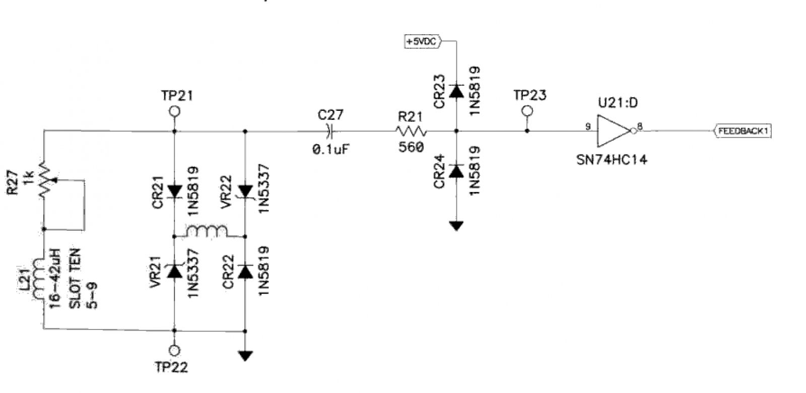 When the tank capacitor is fully charged and the tank begins its journey back down toward zero, the CT signal will begin to fall. When it does, the inverter brings “FEEDBACK1” high and we find ourselves back over to the land of Flip-Flops.With the “FEEDBACK1” signal now high, “PHASE_A” is forced low and “PHASE_B” is forced high, and the IGBT bridge switches gracefully at the zero crossing point, so long as our initial pulse is still high. If for some reason the pulse terminates (which it will in the future), U23:B, the SN74HC74 flip-flop switches low, clears the upper flip-flop and terminates the bridge’s switching.All as long as the “CUR_FAULT” line is held high, that is. If it falls low, the switching is terminated.The current fault detection circuit is shown here in figure S. The second current transformer core’s signal enters this portion of the circuit, and if the positive peak current is too high compared to the reference set by R61, the LM311 comparator switches low, and the switching terminates.I stress positive, because this circuit is only sensitive to the positive peak; and for good reason too. If the current limiting were to kick in on both the positive and negative parts of the cycle, we might miss a phase change and the IGBTs would explode the next time they were switched. This, coupled with the clocked D flip-flop keeps the current fault line held low and the indicator LED held high until the end of our initial, “Let’s Go” pulse.
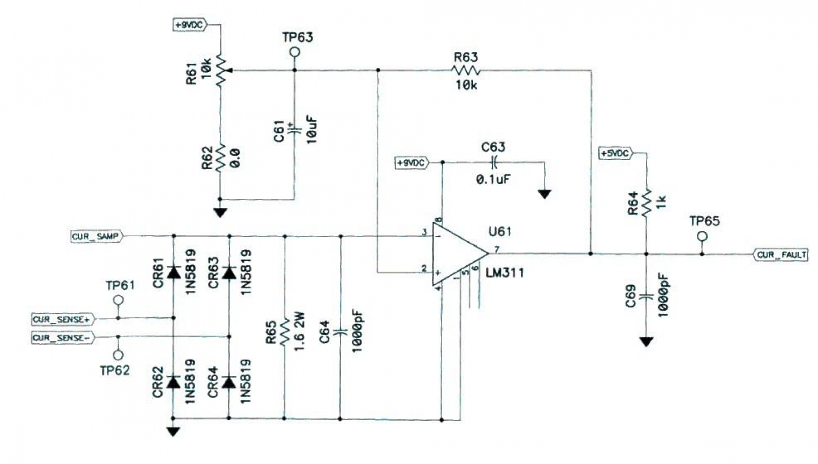 And that’s all there is to it. Simple, elegant, and not a microcontroller anywhere.
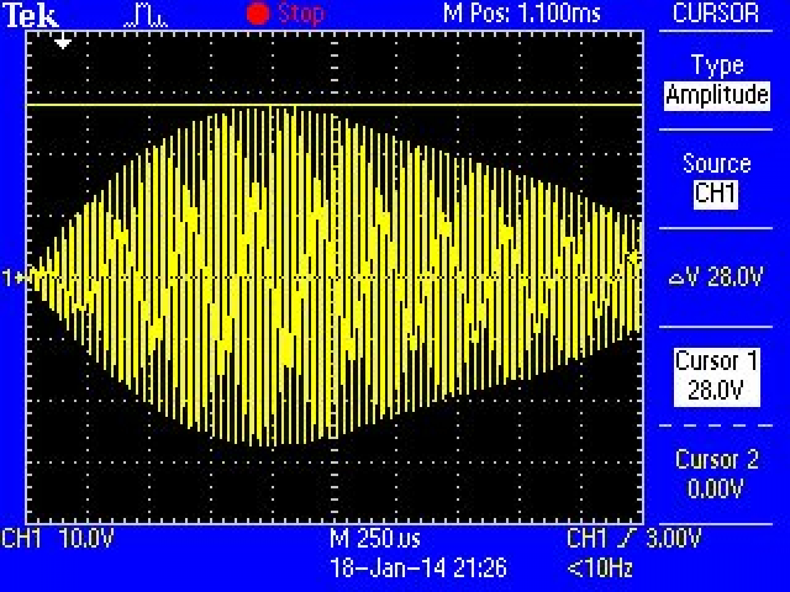 The wavelet begins forming as soon as the bridge begins switching, and its amplitude grows until the switching ceases, where it then begins to dampen. Then, with the bridge no longer active, the freewheeling diodes begin to return energy back into the bus capacitor.Some power is lost of course, but this being a reactive circuit, most of the energy can be recovered. That is one thing which a typical spark gap coil cannot do!Figure U details the primary’s voltage profile. Unlike the current waveform, the voltage across the load is not sinusoidal. Instead, it’s a big mean square wave with all sorts of ringing and overshoot!While there’s nothing wrong with a square wave, ringing is almost always bad; certainly so in this case. If left unchecked, such oscillations could eventually destroy our transistors, if not by over-voltage then by heat.
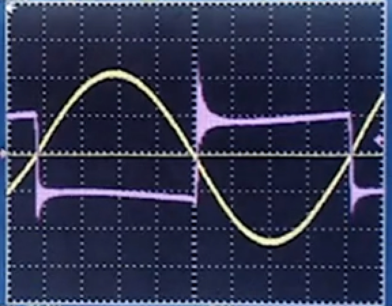 In fact, it’s as simple as adjusting the phase lead inductor. Once timed properly, the IGBTs happily switch at zero crossing and the ringing is gone!There’s still a tiny bit of overshoot left, but nothing to be concerned about.
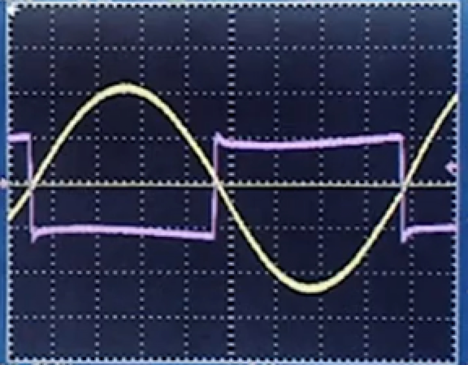 With that all done, it’s time to get sparky (⌐■_■)
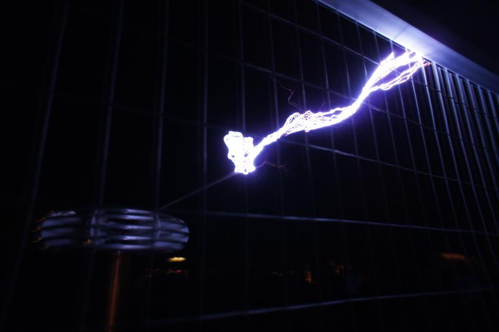
What’s in a coil?
Tesla coils are nothing new, in fact, they have existed for almost 200 years now if one also considers their iron-cored ancestor, the Ruhmkorff coil to be a Tesla coil as well. Nearly everyone has seen one and knows their function; to generate an impressive display of lightning, or, at lower voltages, a large and equally impressive electromagnetic field.In its pure essence, a Tesla coil is nothing more than an inductor and capacitor, tied loosely in resonance with a second, higher inductance, inductor-capacitor “LC tank”. When a spark gap fires, voltage built up in the primary capacitor discharges through the arc and into the primary coil, and depending on how high the system’s quality-factor happens to be, oscillates for up to 100 cycles before the arc gap extinguishes.Theory & Construction
Tesla coils are little else than two resonant LC circuits, as you now know.The simplest way one could turn such a circuit solid state would be to replace the spark gap with an IGBT and suitable snubber network, thereby eliminating losses, light and noise from the gap in one fell swoop. This is impractical though, for two reasons.1. The massive peak currents in the tank, coupled with massive voltage reversal would soon make short order of the IGBT. Realistically, it is impossible to turn off the IGBT again until the oscillation has near completely ceased.2. Apart from eliminating the annoyances of a spark gap, nothing about the coil has really been improved. Rather it’s still the same circuit, just modified a bit. That’s no fun.A more elegant solution would be to use four transistors, or an H-bridge: the same circuit used to control DC motors. By doing so, complete control is available over the primary LC circuit, and fun things can then be done with it. How though, does one build a 1,000 amp, 280V H-Bridge? Very carefully…Here I have the general schema of an H-bridge for such a solid state Tesla coil. For simplicity’s sake, the IGBT flyback diodes have been omitted.LC Tank
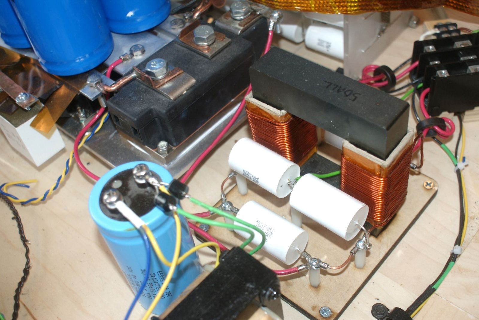
The tank capacitor and primary inductance are kept, at all times resonant. Likewise, the L and C values are matched so that the tank has a very, very low impedance, in my case a whole 4.2 ohms! No matter what way you crunch it, nearly 300V being pumped into a 4.2 ohm circuit such as this one is surely to induce immense currents, which means parasitic currents become a huge issue. Having stray inductances can only foretell oscillatory doom for the poor transistors.To ensure that there is as little stray inductance as possible in the bridge, care must be taken when constructing the device itself. The bus capacitors must, under any and all circumstances be located as close as possible to the transistors. Not only that, but care must be taken when routing the bus-metal, to ensure that no stray inductances prevent the capacitor’s energy from being available when the transistors ask for it. This basically means, no long wires.By mounting capacitors atop the transistors and having bifilar bussing, stray inductances are avoided, and/or canceled out. At 40kHz, the skin depth of aluminum is only about 0.4mm so it’s also critical that bussing be done with wide, flat connections to ensure a low DC resistance.Charging the Tank
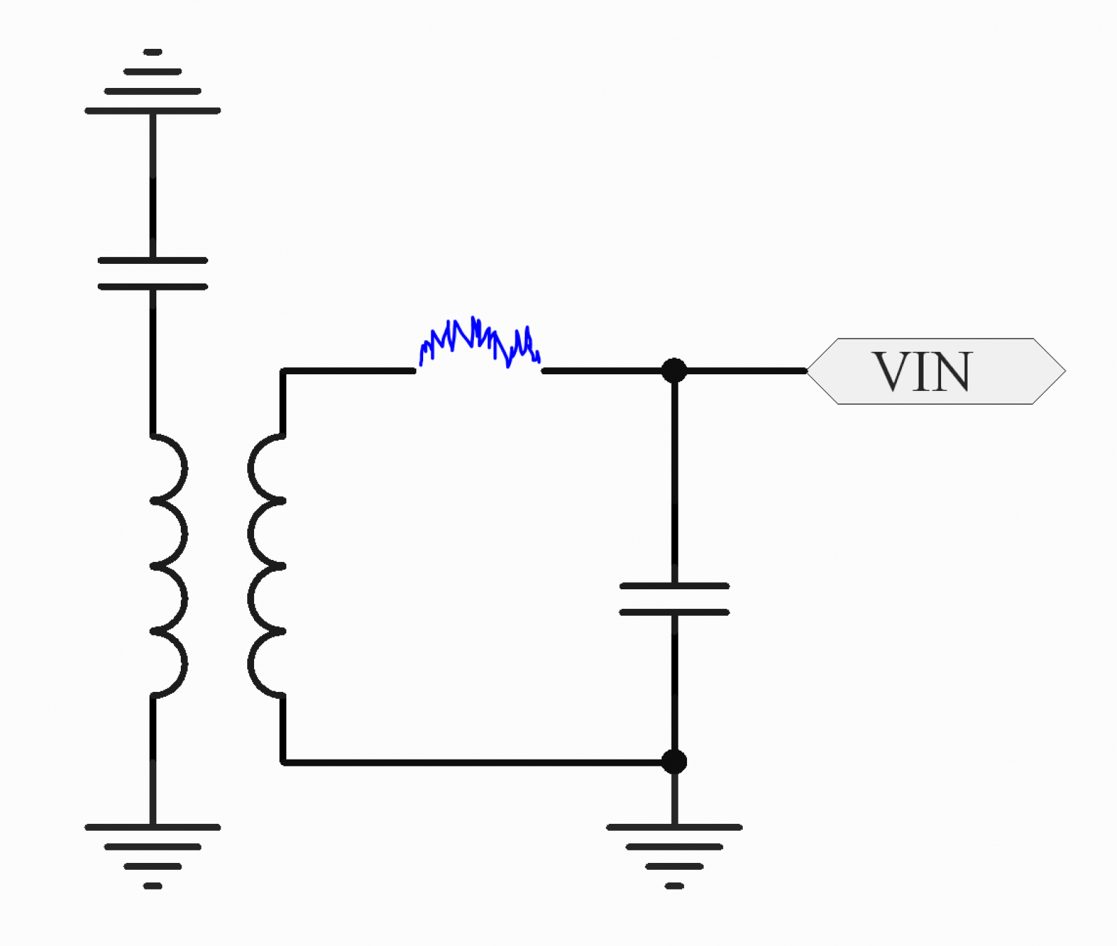
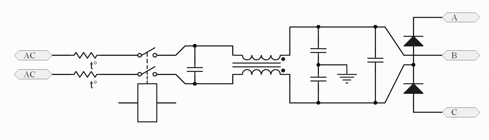
The input to the LC tank is nothing all that special; just a voltage doubler, itself preceded by a common mode EMI filter, a relay and inrush-limiting thermistors. Power is pulled from two phases, giving a final maximum possible bus voltage of (120 * 2 * 1/sin[45]) ~ 280V. Under load this will drop considerably, possibly even as low as to 260V, but this is not a huge concern.Control Circuitry
Controlling such a bridge is no simple task. As sturdy as they may be, any transistor is likely to explode driving such a low impedance if it is run for any more than a few milliseconds’ worth of cycles. Unfortunately then, it is not possible to simply connect up your standard PLL and have it start running on a system like this.Instead, to ensure that the oscillations do not grow destructively large the bridge must only be active for a few hundred microseconds at a time. In doing so, IGBT desaturation is prevented, and the possibility for single-spark control is opened up. But how does one do this, exactly; to start and stop such a large, resonant oscillation at will? Via logic!Results
Here is the tank current developed when one pulse is sent to the coil.